Structures

Overview | Semiconductors| Catalysts | Protection | Structures | Devices| Systems

Goal

Side-view scanning electron micrograph of an array of silicon microwires.1

Make arrays of three-dimensionally structured semiconductors that: 1) maximize absorption of light; and, 2) increase the probability of collecting the oppositely charged carriers generated by the absorption of light; while, 3) minimizing the total volume of the semiconducting material.

Strategy

We employ top-down and bottom-up strategies for structuring semiconductors.

In the top-down approach, we use optical and materials models to determine three-dimensional shapes that will be optimal for absorbing light and collecting photogenerated charge carriers. We then use vapor-liquid-solid growth or etching techniques to fabricate semiconductors, particularly silicon, into the desired shapes.  These techniques produce high-aspect-ratio structures with a long axis that allows absorption of visible light and a short axis that reduces the distance over which charge carriers must travel through the material before being collected.

phototropic_sadtler

Scanning electron micrographs of selenium-tellurium films produced using light-directed growth showing effects of polarization, wavelength, and incident angle on the resulting structure.2

In the bottom-up approach, we allow interactions between light and semiconductors to direct the growth of three-dimensional structures.  Since in this case the growth is a response to the presence of light, the resulting structure is self-optimized for light absorption.  We use photoelectrodeposition to grow the structures from chalcogen oxides dissolved in solution.  We develop and use optical and materials models to understand how interactions between the light and the materials result in the three-dimensional structures we observe.

Growth of three-dimensional semiconductors can also be accomplished using solution-based chemistry.  However, such techniques result in suspensions in which the structures are oriented randomly.  We develop methods for orienting suspended semiconductor structures and for placing the oriented structures into arrays.

Highlights

Effects of Spectral Distribution and Polarization of Optical Inputs on Light-Directed Growth of Selenium-Tellurium Films

Selenium–tellurium films grown via electrodeposition from solutions containing a mixture of selenium oxide and tellurium oxide spontaneously develop ordered, lamellar patterns in response to the presence of light.2

phototropic_polarization_carim

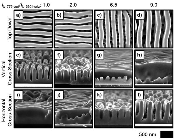
Scanning electron micrographs of selenium-tellurium films grown under simultaneous illumination from a horizontally polarized light source (λavg= 620 nm) and a vertically polarized light source (λavg=775 nm), as a function of relative intensity of the two sources. The relative heights of the two sets of intersecting lamellae depended on the relative intensities of the two light sources.4

The space between the lamellae depends on the illuminating wavelength; polarized light produces patterns aligned with the axis of polarization, and complex three-dimensional structures can be grown by changing the optical inputs during the growth.  The spontaneous structuring of Se-Te films does not require the light source to be a laser, and occurs even when using light that is neither structured physically nor necessarily coherent.


We found that simultaneous illumination from two narrowband sources with different wavelengths results in a structure with a periodicity intermediate between that produced using either of the sources alone.3  The resulting periodicity could be varied by manipulating the relative intensity of the two sources.  Simulations of agreed with experiments, and indicated that self-optimization of the pattern by the growing material resulted in maximization of the anisotropy of interfacial light absorption in the three-dimensional structure.

We also found that simultaneous illumination from two linearly polarized sources with different directions of polarization results in a structure where the long axes of the lamellae are parallel to the intensity-weighted-average of the two polarization orientations.4  Illumination using two orthogonally polarized sources produced structures that consisted of two intersecting sets of orthogonally oriented lamellae.  Simulations were consistent with experimental observations and showed that the lamellae preferentially absorb light polarized with electric field vectors parallel to the long lamellar axes.

Imaging Charge-Carrier Generation in Semiconductor Microwire Arrays


imaging_carrier_generation_sems

Representative scanning electron micrographs of p-type Si microwire arrays decorated by Au photoelectrodeposited from solution using illumination from a narrowband LED having λavg as indicated. The photoelectrodeposited Au appears bright in the images, and is primarily found at the tips of the microwires when short-wavelength illumination is used for the deposition.7

Unlike planar semiconductors, three-dimensionally structured semiconductors can exhibit complex light-absorption profiles that are spatially anisotropic in two or three dimensions.  The optoelectronic and electrochemical properties of silicon microwire arrays and isolated silicon microwires have been experimentally characterized;5–6 however, analyses of the nanoscale processes that are present in microwire arrays and that determine the macroscopic properties of microwire arrays had relied on theoretical and computational methods.


When photoactive semiconductors are immersed in a solution containing metal ions, the optical excitation which results from illuminating the semiconductor can provide the driving force for electrodeposition of a metal.  Because the deposition of the metal is driven by charge carriers generated in response to local absorption of light, the metal deposits only near locations where light has been absorbed.  We applied this principle to image the carrier-generation profiles for arrays of cylindrical or tapered Si microwires, providing an experimental approach for measuring nanoscale processes in three-dimensionally structured semiconductors.7

We used photoelectrodeposition of Au to profile photoinduced charge-carrier generation in illuminated arrays of p-type Si microwires on Si substrates.  We observed that the Au deposited anisotropically onto the microwires, and that the spatial distribution of Au on the microwires was dependent on the wavelength of illumination.  A comparison of the anisoptropic metal-plating profiles obtained for the p-type Si microwire arrays to the conformal metal-plating profiles obtained for illuminated n-type Si microwire arrays provided additional evidence of the dependence of the metal-plating profiles on the carriers generated by the local absorption of light, because the deposition of Au requires electrons to reach the interface with the solution – a dark process for n-type materials but a light-dependent process for p-type materials.

Simulated relative photocarrier-generation rates in Si microwires in arrays and under narrowband illumination with spectral profiles having lavg as indicated.7 The dimensions of the simulated microwires and arrays match those of the microwire arrays shown in the SEMs above.

Simulated relative photocarrier-generation rates in Si microwires in arrays and under narrowband illumination with spectral profiles having λavg as indicated.7 The dimensions of the simulated microwires and arrays match those of the microwire arrays shown in the SEMs above.


The metal-plating profiles were compared to charge-carrier-generation profiles computed using full-wave electromagnetic simulations, and the experimental observations correlated well with the calculated profiles.  The experimental technique demonstrated in this work should be extensible to the determination of spatially resolved carrier-generation profiles in a variety of mesostructured semiconductors.


References

  1. Santori, E. A.; Maiolo, J. R.; Bierman, M. J.; Strandwitz, N. C.; Kelzenberg, M. D.; Brunschwig, B. S.; Atwater, H. A.; Lewis, N. S., Photoanodic behavior of vapor-liquid-solid-grown, lightly doped, crystalline Si microwire arrays. Energy Environ. Sci. 2012, 5 (5), 6867-6871.
  2. Sadtler, B.; Burgos, S. P.; Batara, N. A.; Beardslee, J. A.; Atwater, H. A.; Lewis, N. S., Phototropic growth control of nanoscale pattern formation in photoelectrodeposited Se-Te films. Proc. Natl. Acad. Sci. U.S.A. 2013, 110 (49), 19707-19712.
  3. Carim, A. I.; Batara, N. A.; Premkumar, A.; Atwater, H. A.; Lewis, N. S., Self-Optimizing Photoelectrochemical Growth of Nanopatterned Se–Te Films in Response to the Spectral Distribution of Incident Illumination. Nano Lett. 2015, 15 (10), 7071-7076.
  4. Carim, A. I.; Batara, N. A.; Premkumar, A.; Atwater, H. A.; Lewis, N. S., Polarization Control of Morphological Pattern Orientation During Light-Mediated Synthesis of Nanostructured Se-Te Films. ACS Nano 2015, 10 (1), 102-111.
  5. Xiang, C. X.; Meng, A. C.; Lewis, N. S., Evaluation and optimization of mass transport of redox species in silicon microwire-array photoelectrodes. Proc. Natl. Acad. Sci. U.S.A. 2012, 109 (39), 15622-15627.
  6. Kelzenberg, M. D.; Turner-Evans, D. B.; Kayes, B. M.; Filler, M. A.; Putnam, M. C.; Lewis, N. S.; Atwater, H. A., Photovoltaic measurements in single-nanowire silicon solar cells. Nano Lett. 2008, 8 (2), 710-714.
  7. Dasog, M.; Carim, A. I.; Yalamanchili, S.; Atwater, H. A.; Lewis, N. S., Profiling Photoinduced Carrier Generation in Semiconductor Microwire Arrays via Photoelectrochemical Metal Deposition. Nano Lett. 2016, 16 (8), 5015-5021.

by Kimberly Papadantonakis, June 2016.